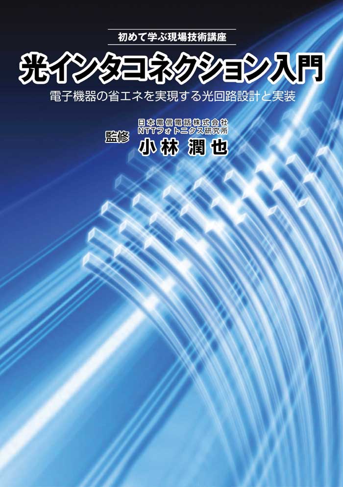
書籍
書籍検索
送料無料

ハンドブックシリーズ

光インタコネクション入門
電子機器の省エネを実現する光回路設計と実装直販のみ

監修: 小林潤也氏(日本電信電話株式会社・NTTフォトニクス研究所)
著者: 青木重憲氏(株式会社富士通研究所)
裏升吾氏(京都工芸繊維大学)
小林潤也氏(日本電信電話株式会社)
近藤 崇氏(富士ゼロックス株式会社)
塩田剛史氏(三井化学株式会社)
宍倉正人氏(日本オプネクスト株式会社)
芝 和宏氏(日本電気株式会社)
長瀬 亮氏(千葉工業大学)
橋本義仁氏(日本電気株式会社)
松原孝宏氏(京セラ株式会社)
定価: 4,400円(本体4,000円+税)
判型: A5
ページ数: 160 ページ
ISBN: 978-4-903242-45-3
発売日: 2010/10/1

【目次】

第1章 光インタコネクションとは

第2章 光データ伝送の基礎

  1. 1 はじめに
  2. 2 光データ伝送の基本構成
    1. 2-1 光電気変換部
    2. 2-2 光伝送路
    3. 2-3 光接続
  3. 3 リンクロスバジェット
  4. 4 おわりに

第3章 光配線

  1. 1 はじめに
  2. 2 光配線板とは
  3. 3 光配線板の動向
    1. 3-1 石英ファイバを用いたフレキシブル光配線板
    2. 3-2 高分子光導波路を用いた光配線板
  4. 4 開発事例(高分子導波路フレキシブル光配線板)
  5. 5 おわりに

第4章 受発光素子

  1. 1 レーザダイオード
    1. 1-1 面発光レーザとは
    2. 1-2 GaAs基板上面発光レーザ
    3. 1-3 InP基板上面発光レーザとGaN基板上面発光レーザ
    4. 1-4 面発光レーザの今後
  2. 2 受光素子
    1. 2-1 はじめに
    2. 2-2 受光素子の動作原理による分類
    3. 2-3 PINフォトダイオードの分類
    4. 2-4 PINフォトダイオードの動作原理および設計のポイント
    5. 2-5 インタコネクション用受光素子の設計ポイント
  3. 3 サブアセンブリ
    1. 3-1 高速光送受信モジュールの種類
    2. 3-2 光実装技術
    3. 3-3 光送受信モジュールの性能指標

第5章 光接続

  1. 1 光結合
    1. 1-1 光接続における主な課題
    2. 1-2 直接結合(端面結合)
    3. 1-3 レンズ結合
    4. 1-4 高効率化・低コスト化と自己形成導波路
    5. 1-5 高密度化の展望
  2. 2 光コネクタ
    1. 2-1 はじめに
    2. 2-2 光コネクタの基本構造
    3. 2-3 光コネクタ技術の流れ

第6章 光導波回路

  1. 1 はじめに
  2. 2 光導波路
  3. 3 光分岐回路
  4. 4 光スイッチ
  5. 5 波長合分波回路

第7章 光インタコネクションの応用例

  1. 1 概要
  2. 2 ハイエンド機器(ルータ/サーバ)
    1. 2-1 スーパーコンピュータへの応用
    2. 2-2 ルーターへの応用
    3. 2-3 将来のデータセンタのサーバへの応用
  3. 3 民生機器への光配線板の応用
    1. 3-1 はじめに
    2. 3-2 光配線板の想定市場
    3. 3-3 携帯機器への応用検討事例
    4. 3-4 実用化への課題
    5. 3-5 おわりに

第8章 光インタコネクション技術の展望

  1. 1 光インタコネクションの技術動向と課題
    1. 1-1 はじめに
    2. 1-2 オンボード光インタコネクション
    3. 1-3 オンボード光インタコネクションの効果
    4. 1-4 オンボード光インタコネクションの実用化に向けた課題[3]
    5. 1-5 将来技術
    6. 1-6 産業としての課題
  2. 2 あるべき姿

【参考文献】

  • 三上修:「光電気実装技術の変遷と将来展望」,電子情報通信学会誌 C,Vol.J92-C,No.8,pp.404-411,2009.
  • 伊賀健一:「フォトニクスの新領域を開いた面発光レーザ」,応用物理学会誌,第78巻,第11号,pp.1060-1066,2009.
  • 篠原弘道:「やさしいファイバ通信」,電気通信協会.
  • 塩田剛史:「光配線技術のすべて」,工業調査会,2007.
  • 小林壮一:「ポリマ導波路の研究開発動向」,エレクトロニクス実装学会誌,Vol.12,No.5,pp.375-380,2009.
  • エレクトロニクス実装学会 光回路実装技術ロードマップWG編:「光インタコネクション普及に向けての提言(光回路実装技術ロードマップWG 2008年度版)」2008.10.
  • 蔵田和彦:「光データ伝送の基礎」,エレクトロニクス実装学会誌,Vol.9,No.1,pp.66-70,2006.
  • 和田一実:「シリコンフォトニクス」,電子情報通信学会誌,Vol.91,No.3,pp.201-205,2008.
  • 日経エレクトロニクス:2005年6月6日号,pp.59-70.
  • J. R. Bautista:“The potential benefits of photonics in the computing platform” , proceeding of SPIE, Vol.5729, pp.1-8, 2005.
  • 塩田剛史:「光配線板のすべて」,工業調査会,2007.
  • 鈴木修司,斎藤和人,増田宏,木下雅夫,茨木修,岡田義邦:「高密度光配線バックプレーン(Ⅱ)」,電子情報通信学会2005年エレクトロニクスソサイエティ大会予稿集,C-3-124,2005.
  • JPCA規格:「高分子光導波路の試験方法」,JPCA-PE02-05-01S-2008.
  • 石井雄三,林剛,碓氷光男,高原秀行:「マイクロレンズアレイを用いた光バンプ実装技術」,第17回エレクトロニクス実装学会学術講演大会講演論文集,pp.255-256,2003.
  • 三上修,内田貞二:「光表面実装技術の進展」,電子情報通信学会論文誌 Vol.J84-C, No.9, pp.715-726, 2001.
  • 伊賀健一,小山二三夫:「面発光レーザの基礎と応用」,共立出版株式会社.
  • N. Nishiyama, C. Caneau, G. Guryanov, M. H. Hu, X. S. Liu, M. J. Li, R. Bhat, and C. E. Zah:“Long-wavelength vertical-cavity surface-emitting lasers on InP with lattice matched AlGaInAs-InP DBR grown by MOCVD”, J. Sel. Topics Quantum Electron., Vol.11. No.5, pp.990-998, 2005.
  • T. H. Lu, C. C. Kao, H. C. Kuo, G. S. Huang, and S. C. Wang:“CW lasing of current injection blue GaN-based vertical cavity surface emitting laser”, Appl. Phys. Lett., Vol.92, 141102, 2008.
  • S.A. Blokhin. J.A. Mutig, G. Fiol, N. N. Ledentsov, M. V. Maximov, A. M. Nadtochiy, V. A. Shchukin, and D. Bimberg:“Oxide-confined 850 nm VCSELs operating at big rates up to 40 Gbit/s” , Electron. Lett., Vol.45, No.10, pp.501-503, 2009.
  • T. Kondo, S. Omori, K. takeda, M. Yoshikawa, A. Murakami, and N. Ueki:“Characterristics and reliability of 10 Gbps/channel 1 x 10 vertical- cavity surface-emitting laser array of 850 nm wavelength”, Jpn. J. Appl. Phys/., Vol.47, pp.6767-6771, 2008
  • 例えば、H. Ishihara, K. Makita, Y. Sugimoto, T. Torikai, and K. Taguchi:“Hugh-temperature aging tests on planner structure InGaAs/InP PIN photodiodes with Ti/Pt and Ti/Au contact”, Electron. Lett., Vol.20, No.16, pp.654-656, 1984.
  • 例えば、K. Taguchi, T. Torikai, Y. Sugimoto, K. Makita, H. Ishihara, S. Fujita, and K. Minemura:“Planner InP/InGaAs avalanche photodiodes with preferential lateral extended guardring”, IEEE Electron. Device Lett., Vol.EDL-7, No.4 pp.257-259, 1986.
  • J. E. Bowers and C. A. Burrus:“Ultrawaide-band long-wavelength p-i-n photodetectors”, IEEE J. Lightwave technol., Vol.LT-5, No.10, pp.1339-1350, 1987.
  • K. Fukatsu, K. Shibata, Y. Suzuki, N. Suzuki, T. Anan, H. Hatakeyama, K. Yashiki, and M. Tsuji:“30 Gb/s over 100-m MFs using 1.1-μm range VCSELs with 35 Gbit/s error-free operation”, IEEE Photon. Technol. Lett., Vol.20, No.11, pp.909-910, 2007.
  • 吉村学:「TOSA,ROSA,トランシーバ回路」,光配線実装技術ハンドブック,オプトロニクス社,pp.198-202,2008.
  • K. Giboney, P. Rosenberg, A. Yuen, J. Straznicky, S. Corzine, L. Buckman, D. Dolfi:“The PONI optoelectronic platform”, Lasers and Electro-Optics Society 1999 12th Annual Meeting., Vol.1, pp.25-26, 1999.
  • K. Katsura, M. Usui, M. Hikita, R. Yoshimura, and Y. Ando:“Packaging for a 40-channel parallel optical interconnection module with an over-25-Gbit/s throughput”, Advanced Packaging, IEEE Transactions on, Vo;.22, No.4, pp.551-560, 1999.
  • 畠山意知郎,三好一徳,樋野智之,清水隆,佐々木純一,山本圭介,栗原充,蔵田和彦:「光I/O内蔵システムLSIモジュールによる高速光インタコネクション」,電子情報通信学会,第6回システムフォトニクス研究会,pp.35-39,2004. 7.
  • Daikuhara, Aoki, and Takauchi:“An optcal parallel transceiver with polymeric three dimensional waveguide”, IEICE technical report. EMD 106(212), pp.99-102, 2006.
  • 高原秀行,石橋重喜,石沢鈴子,平田泰興,小勝負信建,恒次秀起:“OE-COF(Optoelectronic Chip on Film)実装技術の検討”,信学論 C,vol.J84-C, pp.800-806, 2001.
  • M. Mikawa, M. Kinoshita, K. Hiruma, T. Ishitsuka, M. Okabe, S. Hiramatsu, H. Furuyama, T. Matsui, K. Kumai, O. Ibaraki, and M. Bonkohara, “Implementation of active interposer for high-speed and low-cost chip level optical interconnects”, IEEE J. Select. Top. Quantum Electron., vol.9, pp.452-459, 2003.
  • T. Okayasu, D. Watanabe, A. Ono, M. Shibata, Y. Hayase, T. Shirai, T. Inoue, K. Ueno, F. Hosoi, T. Akiyama, “Direct current to 34.1-Gb/s, 19-Gb/s/cm3 low-jitter parallel optical interconnecting module for high-speed memory test systems”, J. Lightwave Techcnol., Vo;.22, pp.2064-2082, 2004.
  • T. Matsubara, K. Oba, K. Watanabe, K. Tanaka, M. maetani, Y. Nishimura, and S. Tanahashi:“Three dimensional optical interconnect on organic circuit board“, Proc. 56th Electron. Compo. Technol. Conf., pp.789-794, May 30-June 2, 2006.
  • H. Hamasaki, H. Furuyama, H. Numata, and C. Takubo:“Novel optoelctronic LSI packaging suitable for standard FR-4 printed wiring board with bandwidth capability of over 1 Tbps”, Proc. 56th Electron. Compo. Technol. Conf., pp.298-302, May 30-June 2, 2006.
  • A. L. Glebov, C. J. Uchibori, and M. G. Lee, “Direct attach of photonic components on substrates with optical interconnects”, IEEE Photon. Technol. Lett., Vol.19, pp.547-549, 2007.
  • 石井雄三,新井芳光:「チップレベル光インタコネクションのための広トレランス"光バンプ”インタフェース」,信学論 C,vol.J84-C, pp.793-799, 2001.
  • L. Schares, J. A. Kash, F. E. Doany, C. L. Schow, C. Schuster, D. M. Kuchta, P. K. Pepeljugoski, J. M. Trewhella, C. W. Baks, R.A. John, L. Shan, Y. H. Kwark, R. A. Budd, P. Chiniwalla, F. R. Libsch, J. Rosner, C. K. Tsang, C. S. Patel, J. D. Schaub, R. Dangel, F. Horst, B. J. Offrein, D. Kucharaski, D. Guckenberger, S. Hegde, H. Nyikai, C-K. Lin, A. Tandon, G. R. Trott, M. Nystrom, D. P. Bour, M. R. T. Tan, and D. W. Dolfi:“Terabus:Terabit/second-class card-level optical interconnect technologies”, IEEE J. Select. Top. Quantum Electron., Vol.12, pp.1032-104, 2006.
  • M. Karppinen, T. Alajoki, A. Tanskanen, K. Kataja, J. -T. Makinen, K. kauto, P. Karioja, M. Immonen, J. Kivilahti, and A. Oy:“Parallel optical interconnect between ceramic BGA packages onFR4 board using embedded waveguides and passive optical alignments”, Proc. 56th Electron. Compo. Technol. Conf., pp.799-794, May 30-June 2, 2006.
  • M. Shishikura, Y. Matsuoka, T. Ban, T. Shibata, and A. Takahashi:“A high-coupling-efficiency multilayer optical printed writing board with a cube-core structure for high-density optical interconnection”, Proc. 57th Electron. Compo. Technol. Conf., pp.1275-1280, May 29-June 1, 2007.
  • T. Hino, R. Kuribayashi, Y. Hashimoto, T. Sugimoto, J. Ushioda, J. Sasaki, I. Ogawa, I. Hatakeyama, and K. Kurata:“A 10 Gbps x 12 channel pluggable optical transceiver for high-speed interconnection”, Proc. 58th Electron. Compo. Technol. Conf., pp.1838-1843, May 27-30 , 2008.
  • M. Kagami, T. Yamashita, and H. Ito:“Light-induced self-written three-dimensional optical waveguide”, Appl. Phys. Left., vol.79, pp.1079-1081, 2001
  • M. Miler and M. Skalsky:“Stigmatically focusing grating coupler“, Electron Lett., Vol.15, pp.275-276, 1979.
  • S. Ura, K. Shinoda, K. kintaka, C.Ito, D. Nii, K. Nishio, and Y. Awatsuji,:“Giga-bits/second signal transmission from single mode VCSEL via thin-film waveguide for WDM optical interconnects board”, Jpn. J. Appl. Phys., Vol.47, pp.6664-6666, 2008.
  • 金高健二,西井準治,山口智史,裏升吾:「チャネル光導波路を用いたボード内チップ間波長多重光配線の提案」,信学論 C,vol.J90-C, pp.767-774, 2007.
  • N. Suzuki, Y. Iwahata, M. Saruwatari, and K. Nawata:“Ceramic capillary connector for 1.3μm single-mode fibers”, Electron. Lett., Vol.15, No.25, pp.809-811, 1979.
  • N. Suzuki, M. Saruwatari, and M. Okuyama:“Low insertion-and high return-loss optical connectors with spherically convex-polished end”, Electron. Lett., Vol.22, No.2, pp.110-112, 1986.
  • E. Sugita, R. Nagase, K. Kanayama, and T. Shintaku:“SC-type single-mode optical fiber connectors”, IEEE J. Lightwave Technol., Vol.7, No.11, pp.1689-1696, 1989.
  • S. Nagasawa, H. Fukuhara, M. Makita, and H. Murata:“Mechanically transferable single-mode multifiber connectors”, Proc. Integrated Optics and Optical Fiber Commun. ’89, 21C2-1, pp.48-49, 1989.
  • S. Nagasawa, Y. Yokoyama, F. Ashiya, and T. Satake:“A high-performance single-mode multifiber connector using oblique and direct endface contact between multiple fibers arranged in a plastic ferrule”, IEEE Photon. Technol. Lett., Vol.3, No.10, pp.937-939, 1991.
  • R. Nagase, E. Sugita, S. Iwano, K. Kanayama, and Y. Ando:“Design for MU-type single-mode miniature optical connector”, IEICE Trans. Electron. Vol.E81-C, No.3, pp.408-415, 1998.
  • M. A. Shahid, N. R. Lampert, A. W. Carlisle, D. A. Hendrickson, D. M. Emmerich, T. E. McNeil, and J. E. George:“Small and efficient connector system”, un Proc. 49th Electron. Comp. Technol. Conf., San Diego, CA, pp.375-380, June 1999.
  • 岡本勝就:「光導波路の基礎」,コロナ社,1992.
  • N. Takako, K. Jinguji, M. Yasu, H. Toba, and M. Kawachi:“Silica-based single-mode waveguides on silicon and their application to guided-wave optical interferometers”, IEEE J. Lightwave Technol., Vol.6, No.6, pp.1003-1010, 1988.
  • J. Kobayashi, T. Matsuura, S. Sasaki, and T. Maruo:“Directional couplers using fluorinated polyimide waveguides”, IEEE J. Lightwave Technol., Vol.16, No.4, pp.610-614, 1998.
  • S. Suzuki, M. Yanagisawa, Y. Hibino, and K. Oda:“High-density integrated planar lightwave circuits using SiO2-GeO2 waveguides with a high refractive index difference ”, IEEE J. Lightwave Technol., Vol.12, No.5, pp.790-796, 1994.
  • 鈴木扇太,河内正夫:「石英系プレーナ光波回路」,電子情報通信学会論文誌,J77-1C-1,pp.184,1994.
  • A. sugita, K. Jinguji, N. Takako, K. Katoh, and M. Kawachi:“Bridge-suspended silica-waveguide thermo-optic phase shiffer and its application to Mach-Zehnder type optical switch”, Trans. IEICE, Vol.E73-E, No.1, pp.105-109, 1990.
  • J. Kobayashi, T. Matsuura, Y. Hida, S. Sasaki, and T. Maruo:“Fuorinated polyimide waveguides with low polarization -dependent loss and their applications to thermooptic switche”, IEEE J. Lightwave Technol., Vol.16, No.6, pp.1024-1029, 1998.
  • M. K. Smit:“New focusing and dispersive planar component based on an optical phased array”, Electron. Lett., Vol.24, No.7, pp.385-386, 1988.
  • H. Takahashi, K. Oda, H. Toba, and Y. Inoue:“Transmission characteristics of arrayed waveguide N × N wavelength multiplexer”, IEEE J. Lightwave Technol., Vol.13, No.3, pp.447-455, 1995.
  • J. Kobayashi, Y. Inoue, T. Matsuura, and T. Maruo:“Tunable and polarization-insensitive arrayed-waveguide grating multiplexer fabricated from fuorinated polyimides”, IEICE, Trans. Electron., Vol.E81-C, No.7, pp.1020-1026, 1998.
  • Y. Inoue, T. Oguchi, Y. Hibino, S. Suzuki, M. Yanagisawa, K. Moriwaki, and Y. Yamada:“Filter-embedded wavelength-division multiplexer for hybrid-integrated transceiver based on silica-based PLC”, Electron. Lett., Vol.32, No.9, pp.847-848, 1996.
  • 宍倉正人:「光伝送技術の導入と電気変換部の発展」,エレクトロニクス実装学会誌,第9巻,第2号(通巻第57号),pp.123,2006.3.
  • T. Okayasu, D. Watanabe, A. Ono, M. Shibata, Y. Hayase, T. Shirai, T. Inoue, K. Ueno, F. Hosoi, and T. Akiyama:“Direct current to 34.1-Gb/s, 19-Gb/s/cm3 low-jitter parallel optical interconnecting module for high-Speed memory test systems”, IEEE J. Lightwave Technol., Vol.22, No.9, pp.2064-2082, 2004.
  • 佐藤達夫:「次世代スーパーコンピュータを実現する光インタコネクション技術」,応用物理,第76巻,第11号,pp.1232-1237,2007.
  • J. A. Kash, F. E. Doany, C. L. Schow, R. Budd, C. Baks, D. M. Kuchta, P. Pepeljugoski, L. Schares, R. Dangel, F. Horst, B. J. Offrein, C. K. Tsang, N. Ruiz, C. Petel, R. Horton, F. Libsch, and J. U. Knickerbocker:“Terabus:chip-to-chip board-level optical data buses”, Proc. LEOS 2008, pp.515-516, 2008.
  • Juniper Networks 社 Tシリーズ・ルーティング・プラットフォーム(http://www.juniper.net/jp/jp/local/pdf/datasheets/1000051-jp.pdf).
  • 「通信容量3テラbpsの光バックプレーン(光配線板)を開発」(http://www.aist.go.jp/aist_j/press_release/pr2005/pr20050915_2/pr20050915_2.html).
  • 光テクノロジーロードマップ報告書(情報通信分野)「省エネに貢献するネットワーク技術」,光産業技術振興協会,2008.3. (http://www.computerworld.jp/topics/datac/106849.html).
  • “An overview:The next generation of Ethernet”, IEEE 802.3 Higher Speed Study Group - TUTORIAL. (http://www.ieee802.org/3/hssg/public/nov07/index.htm).
  • “40G Ethernet market potential” (http://www.ieee802.org/3/hssg/public/apr07/hays_01_0407.pdf).
  • E. Mohammed, A. Alduino, T. Thomas, H. Braunisch, D. Lu, J. Heck, A. Liu. I. Young, B. Barnett, G. Vandenton, and R. Mooney:“Optical interconnect system integration for ultra-short-reach application”, Intel Technology Journal, Vol.8, pp.114-129, 2004.
  • 「10Gビット/秒のシステム設計で直面するマイクロ波の世界」(http://www.ednjapan.com/content/issue/2006/06/content05.html).
  • H. Chao, P. Kapur, and K. C. Saraswat:“Power comparison between high-speed electrical and optical interconnects for inter-chip communication”, IEEE J. Lightwave Technol., Vol.22, No.9, pp.2021-2033, 2004.
  • J. F. Bulzacchelli, M. Meghelli, S. V. Rylov, W. Rhee, A. V. Rylyakov, H. A. Ainspan, B. D. Parker, M. P. Beakes, A. Chung, T. J. Beukema, P. K. Pepeljugoski, L. Shan, Y. H. Kwark, S. Gowda, and D. J. Friedman:“A 10-Gb/s 5-tap DFE/4-tap FFE transceiver in 90-nm CMOS technology”, IEEE J. Solid-State Circuits, Vol.41, No.12, pp.2885-2900, 2006.
  • 柳町成行,中野嘉一郎,蔵田和彦:「光インタコネクション技術の最新動向」,電子情報通信学会ソサイエティ大会,BS-10,2008.
  • F. E. Doany, C. L. Schow, C. K. Tsang, N. Ruiz, R. Horton, D. M. Kuchta, C. S. Patel, J. U. Knickerbocker, J. A. Kash:“300-Gb/s 24-channel bidirectional Si carrier transceiver optchip for board-level interconnects”, Proc. ECTC 2008, pp.238-243, 2008.
  • 光電子回路実装標準化委員会 普及促進データベース(http://www.jpca.net/hikari/gkr6.html).
  • 塩田剛史:「光配線板のすべて」,工業調査会,2007.9.
  • 松井快成:「光テスター:光配線板用光導通検査装置の提案」,エレクトロニクス実装学会,第38回OPT公開研究会,2009.1.
  • 特願 2006-322349(公開 2008-134211)
  • 光電子回路実装標準化委員会ホームページ(http://www.jpca.net/hikari/top.html)
  • 松原孝宏,小田恵子,渡辺啓一郎,田中香織,前谷麿明:「オンボード光インタコネクションに向けた三次元光配線」,エレクトロニクス実装学会誌,Vol.12,No.5,pp.440-445,2009.8.
  • 柳町成行,栗林亮介:「低消費電力光インタコネクション」,エレクトロニクス実装学会誌,Vol.12,No.5,pp.434-439,2009.8.
  • エレクトロニクス実装学会 光回路実装ロードマップWG編:「光インタコネクション普及に向けての提言(光回路実装ロードマップWG 2008年度版)」,2008.10.
  • 裏升吾,村田博司:「広帯域波長多重光配線板」,光配線実装技術ハンドブック,第3章,オプトロニクス社刊,2008.9.
  • 山田浩治:「シリコンフォトニクス」,光配線実装技術ハンドブック,第5章,オプトロニクス社刊,2008.9.

【口コミ】

  • ※口コミはありません。
ページトップへ戻る